Faculty of Electronics and Computer Sciences, Koszalin University of Technology, ul. Śniadeckich 2, 75-453 Koszalin, Poland
Institute for Electronic Structure Dynamics, Helmholtz-Zentrum Berlin für Materialien und Energie GmbH,
Albert-Einstein-Strasse 15, 12489 Berlin, Germany
Department of Chemistry, Humboldt-Universität zu Berlin, Brook-Taylor-Strasse 2, 12489 Berlin, Germany
Leibniz-Institut für Kristallzüchtung (IKZ), Max-Born-Strasse 2, 12489 Berlin, Germany
Department of General Physics, Lviv Polytechnic National University, 12 Stepan Bandera St., 79013 Lviv, Ukraine
Article Info
Received 05 Sep. 2024
Received in revised form 07 Dec. 2024
Accepted 12 Dec. 2024
Available on-line 27 Jan. 2025
Keywords: semiconductors;
doped silicon crystals;
far-infrared reflection spectra;
free electrons;
electron momentum scattering time;
effective mass of electron.
The reflection spectra of n- and p-type silicon crystals doped with phosphorus and boron
were measured for the free carrier concentrations of 1.1 · 1015 cm-3 − 1.2 · 1020 cm-3 in the
far- and mid-infrared range between 20–3000 cm-1 using synchrotron radiation and Fourier
transformed infrared technique. Transmittance spectra could be measured for lower sample
carrier concentrations from the range studied. The measured reflection spectra were fitted
by using the Drude relation and the parameters of free electron conductivity (electron
effective mass m* and momentum scattering time τ) were obtained for the n- and p-typedoped
silicon. Additionally, the calculations of the band electronic structure and the electric
conductivity σ of the crystals were performed in the framework of the density functional
theory for different carrier concentrations and temperatures. The study main findings are (1)
the substantial decrease of the momentum scattering time τ and (2) the clear increase of the
electron effective mass m* with an increase of the carrier concentrations Nc for both n- and
p-type-doped silicon crystals.
Introduction
Doping plays a key role in all electronic devices, as all basic
parameters of such devices are affected by dopant distributions.
Doping refers to introducing impurity atoms in
a controlled way to define the electrical properties in
semiconductor materials (usually III and V group species).
The donors and acceptors modify the electron and hole
concentration from 1013 to 1021 cm-3. The carrier concentration
can also be spatially distributed to create pn-junctions
and produce built-in electric fields. Most semiconductor
devices use impurities (dopants) as a crucial ingredient to
modify the electronic and optical properties, as well as the
device structure [1].
Doping of semiconductors allows the manipulation of
their electrical conductivity by exploiting the doping
properties of the chemical elements in the main crystal
matrix. By introducing a limited number of doping
elements into the nominal crystal matrix, the conductivity
of semiconductors can be significantly increased. The main
challenges in this field are (1) ensuring the ability to control
electrical conductivity by controlling the bandgap Eg and
(2) ensuring the maximum mobility of free carriers
(electrons or holes) [2]. Doping is critical to semiconductor
devices, from transistors to thermoelectric energy
converters. The interaction between electrons and
impurities plays a key role in the transport of carriers. It
turns out that high mobility of charge carriers can be
achieved by properly selecting dopant elements to obtain
high mobility in electronic, photonic, and energy
conversion applications [3]. The n- and p-doped silicon
crystals are widely used to fabricate different optoelectronic
devices. That is why deepening the knowledge
of their electronic structure is of interest. The commonly
used substitutional doping of different elements, such as
carbon, chalcogens, and phosphorus, induces various
effects on silicon crystal structural, electronic, and optical
properties [4–7].
It is known that the character of the temperature
dependence of the electric conductivity (metal-like or
semiconductor-like) of an extrinsic semiconductor depends
on the concentration of residual carriers. A metal‑like
character occurs for relatively high carrier concentrations,
while a semiconductor‑like type is observed for relatively
low carrier concentrations. This substantiates an approach
in which the residual carriers may be divided into two parts:
(1) the quasi-free and (2) the weakly bonded carriers. The
quasi-free carriers are responsible for the metal-like electric
conductivity, while the weakly bonded carriers correspond
to the semiconductor-like one. The binding energy
(eigenfrequency) of the quasi-free carriers is taken to be
close to zero (ω01 = 0), whereas the bonded ones may be
characterised by one non-zero binding energy (ω02 ≠ 0). In
this case, the Drude-Lorentz model of the frequency
dependence of dielectric permittivity ε(ω) for electrons in
a doped semiconductor may be presented in the following
form:
where ε∞ is the high-frequency dielectric permittivity, ωp1
and ωp2 are the plasma frequencies, ω02 is the
eigenfrequency of the bonded electrons/holes, and γ1 and γ2 are the damping coefficients [8].
Investigations of the optical reflection and transmittance
spectra of the pure and doped silicon crystals and
associated properties of the quasi-free carriers (electrons
and holes) are widely presented in the literature. Among
these studies, systematic investigations of the carrier
momentum scattering times/damping coefficients and the
electron effective mass in the relatively wide range of free
carrier concentrations, 1015 − 1021 cm-1, are not numerous.
This is partly caused by a relatively small intensity of the
frequently used globar light sources in the far-infrared
range of λ > 15 μm. In the present study, the optical
reflection and transmittance spectra were obtained using
synchrotron radiation, which was much brighter in the farinfrared
range of λ > 15 μm than the globar sources. This
allowed for more valid reflection spectra of doped silicon
crystals with relatively small carrier concentrations,
1015 − 1017 cm-1.
The present study aims to deepen the knowledge of the
electron/hole parameters of the doped silicon crystals in the
relatively wide range of the free carrier concentrations,
1015 − 1021 cm-1, by using the reflection/transmittance
spectra in the far-infrared range of 20–3000 cm-1 obtained
by using the synchrotron radiation. In this range, electrons
are excited from doping states into conduction bands or
from valence bands into acceptor states of the
semiconductor. The results may be useful for practical
applications of silicon crystals in microelectronics and
optoelectronics.
Fourier transformed infrared (FTIR) spectroscopy is an
accurate tool for precise measurements of the reflection and
transmittance spectra. Assuming that reflection and
transmittance of the sample obey the Fresnel’s formula,
several electron- and phonon-related values of the crystals
under study can be obtained, which will be helpful in the
following discussion and conclusions
Experimental
The samples used in this study were 15 × 15 × 0.45 mm3.
The thin plates were cut from the crystals mostly grown by
the floating zone (FZ) technique (see Table 1 for details)
and doped during the growth process using Phosphine for
n-type and Diboran for p-type crystals. Some crystals under
study with higher dopant concentrations were grown using
the Czochralski technique (CZ). The surface orientation of
all samples was (100). Four probe measurements at room
temperature determined the samples resistivity.
Plasma frequency ωp vs. free electron concentration Nc calculated using (2) for ε∞ = 4.0 and m* = 1.0 m0 (m0 is the free electron mass).
Nc /cm-3
ωp /cm-1
1 · 1015
29.7
1 · 1016
94.1
1 · 1017
297
1 · 1018
941
1 · 1019
2976
1 · 1020
9410
1 · 1021
29758
The specular reflection of the doped silicon samples
was taken at an incidence of 8° close to normal and with an
opening angle of about 50 msr. A custom-built motorized
reflection set-up for the spectrometer sample compartment
was used and spectra were taken with a Vertex 70/v FTIR
(Bruker) spectrometer in vacuum in the 20–3000 cm-1 frequency range. A highly intense and brilliant synchrotron
radiation at the IRIS beamline [9] from the BESSY II
electron storage ring of the Helmholtz-Zentrum Berlin
(HZB) was applied as a source.
According to the Drude model of conductivity, the
plasma frequency ωp = ωp1 (1) of the doped semiconductors
depends strongly on the free-carrier (electron or holes)
concentration Nc:
where e is the electron charge, ε0 is the dielectric constant,
ε∞ is the dielectric permittivity caused by the bonded
electrons, m* is the effective mass of the charge carriers in
a semiconductor [10]. To see the quantitative values, Table 1 presents a numerical correspondence between the
plasma frequency ωp and the electron concentration Nc,
according to (2), taking the free electron mass, m0, as the
effective mass, m* = m0. Plasma frequency for freeelectron
concentration below 1 · 1015 cm-3 can reach the
lower limit of the spectral range of the FTIR spectrometer
and therefore is not experimentally accessible by the
spectroscopic method applied in this study.
By fitting the measured reflection spectrum R(ω) of the
doped silicon crystals by (1) using the RefFIT software
[11], the plasma frequency ωp1 and the dissipation coefficient γ1 can be obtained. Afterward, the effective
mass of electrons/holes m* in the doped silicon crystals of
the known carrier concentration Nc can be calculated from
the fitted plasma frequency ωp using (2) [8, 12].
First-principle calculations
Calculations of the electronic properties of the silicon
crystals studied were performed in the framework of the
density functional theory (DFT) using the Vienna ab initio
simulation package (VASP) code [13–18]. Based on the
generalized gradient approximation, the standard Perdew-
Burke-Ernzerhof (PBE) exchange-and-correlation function
[19] has been used.
To calculate silicon crystals electronic properties,
a silicon crystal structure with cubic space group of
symmetry Fd-3m (no. 227) was used.
The calculations were performed by VASP using
projector-augmented wave PBE (PAW_PBE) pseudopotentials,
xc-functional PBE, and a cut-off energy of
500 eV for electron plane waves. One of the calculated
values was the dielectric permittivity ε∞ (dielectric
permittivity caused by bonding electrons). A 3 × 3 × 3
silicon supercell containing 216 atoms was used to
calculate the dielectric permittivity ε∞. The effective
electron mass m* and the corresponding electric
conductivity of the n- and p-type silicon crystals were
calculated within the constant relaxation time
approximation using the AMSET software [20] developed
based on VASP and BoltzTraP2 codes [13–18, 21]. The
authors’ calculations using the AMSET code used eight Si
atoms in the unit cell (1 × 1 × 1) of a pure silicon crystal
(a = b = c = 5.44 Å).
Results and discussion
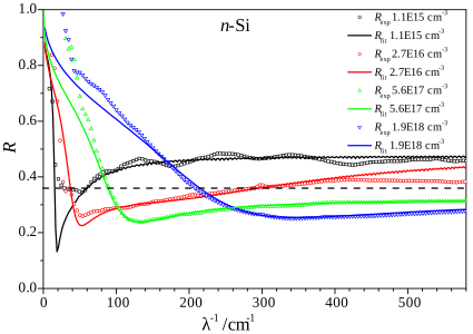
The obtained experimental specular reflection spectra of
doped silicon crystals are shown in Fig. 1. In these
reflection spectra, the authors did not find the features that
can be associated with excitations of bonded electrons or
phonons. Therefore, the fitting of the experimental
reflection spectra was performed using only free electrons,
which means using only the first two members in the right
part of (1):
Fig. 1. Experimental (points) and fitted (lines) specular reflectance spectra of (a) n- and (b) p-doped R(λ−1) silicon single crystals
in the infrared range for different concentrations of Nc carriers, indicated by different colours. Horizontal dashed line
indicates the reflection coefficient R = [(n − 1/n + 1)]2 corresponding to the refractive index of a silicon single crystal caused
by bonded electrons, n = 3.6 (ε∞) = 12.96) for the wavelength λ = 1 μm [22].
In Table 2, the parameters of (2) and (3), ε∞, ωp, γ, and
m*, calculated by the RefFIT package based on the
measured reflectance spectra R(1/λ) of the samples, are
dependent on the free carrier concentration Nc. A slight
decrease of the dielectric constant ε∞ observed with an
increase of the free carrier concentration Nc (Table 2) may
be caused by the screening of the light wave electric field
by free electrons in the doped silicon crystals.
Parameters derived from the fitting of the reflection spectra of n- and p-type-doped silicon single crystals of different carrier
concentrations Nc using (2) and (3) and the RefFIT software [12]. The carrier momentum scattering time τ is proportional to
the inverse damping coefficient γ in (1) and (3), τ = 1/(γc), where c is the light velocity in vacuum.
Doping type/growth technique
Nc,
cm-3
ε∞
ωp,
cm-1
γ, cm−1
τ, s
m*, m0
n / FZ
1.1 · 1015
12.96
61.7
4.52
7.38 · 10-12
0.079
n / FZ
2.7 · 1016
12.96
155
27.3
1.22 · 10-12
0.308
p / FZ
5.8 · 1016
12.96
192
58.0
5.75 · 10-13
0.429
n / FZ
5.6 · 1017
12.96
379
79.3
4.20 · 10-13
1.066
n / FZ
1.9 · 1018
12.96
952
246
1.35 . 10-13
0.574
p / CZ
8 · 1018
12.96
1754
459
7.26 · 10-14
0.712
p / FZ
1.8 · 1019
12.96
2644
543
6.14 · 10-14
0.705
p / CZ
1.2 · 1020
12.96
5984
775
4.30 · 10-14
0.918
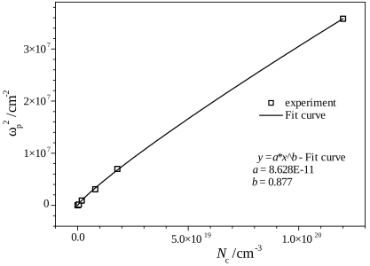
The experimental dependence of the square of plasma
frequency ωp 2 on the carrier concentration Nc reveals the
nonlinear character, which can be fitted sufficiently well by
the allometric function y = a · xb, with the coefficient b less
than unity [b = 0.877, see Fig. 2(a)]. Considering (2) and
the fitted coefficient b < 1, one can conclude that the
monotonous increase of the effective mass m* occurs at the
increase of the carrier concentration Nc.
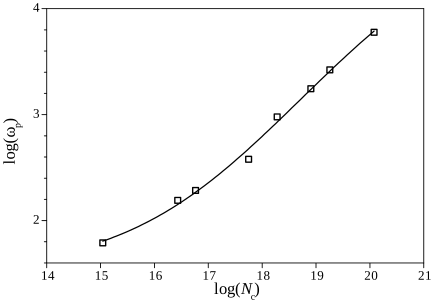
Fig. 2. (a) Dependences of the square of the plasma frequency ωp 2 on the free carrier concentration Nc in the form of experimental points
(Table 2) and a dashed curve (fitting the dependence of ωp
2(Nc) to the power-like function y = a · xb) for the doped silicon crystals;
(b) log-log dependence of the plasma frequency ωp on the free carrier concentration Nc in the form of experimental points (Table 2)
and a solid curve [fitting the dependence ωp(Nc) to the logistic function y = A2 + (A1 − A2)/(1 + (x/x0)p] for the doped silicon crystals.
However, this fitting may not be sufficiently precise in
all regions of the wide carrier concentration range of
1015 − 1021 cm-3. To overcome this drawback, one can (1)
use the double logarithmic scales for Nc and ωp and (2) use
a more complicated function containing more than two
fitting parameters. Taking into account the latter comments,
the fitting of the dependence ωp(Nc) is realized in the double
logarithmic scales using the logistic function containing
four fitting parameters, y = A2 + (A1 − A2)/(1 + (x/x0)p)
[Fig. 2(b)].
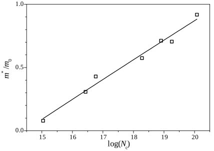
Having obtained the dependence ωp(Nc) [Fig. 2(b)], the
corresponding dependence of the effective electron masses
m* on the free carrier concentration Nc is calculated using
(2) and presented in Table 2 and Fig. 3. In Fig. 3, the point
corresponding to the electron carrier concentration
Nc = 5.6 · 1017 cm-3 (Table 2) is omitted because of the
substantial difference between the experimental and fitted
reflection spectra in Fig. 1(a). The latter circumstance
could cause a large deviation of the effective mass m* from
the fitted linear dependence m*(log(Nc)) in Fig. 3. In the
relatively wide range of the carrier concentration of
1015−1020 cm-3, the dependence m*(log(Nc)) in Fig. 3 is
very close to linear. The second order polynomial fitting of
the experimental dependence m*(log(Nc)) (points in Fig. 3)
, allows the estimation of the effective electron mass m* of
the carriers in doped silicon crystals in a relatively wide
range of carrier concentration of 1015−1020 cm-3.
Fig. 3. Dependences of the effective electron mass m* on the free
carrier concentration Nc for the doped-silicon crystals
obtained on the basis of the experimental far-infrared
reflection spectra (squares – before fitting, solid line –
after fitting).
The values of the effective electron mass of the doped
silicon m* in the carrier concentration range of
1 · 1018 − 5 · 1020 cm-3 obtained from the authors’ experimental
reflection spectra by using the Drude model (2),
m* = 0.7 m0 (Table 2 and Fig. 3), are larger than the
reference data m* = 0.3 m0 [23] for the corresponding
concentration Nc. One of the possible reasons for this
effective electron mass difference may be a different
quality of the corresponding silicon samples, which can
result in different values of the dielectric permittivity ε
∞.
However, the latter point is not considered in some cases
[24–26]. The authors have performed DFT calculations for
pure silicon crystal and heavily phosphorus-doped silicon
crystals (Nc = 5 · 1022 cm-3) corresponding to one phosphorus
and 215 silicon atoms in the supercell and they have found
the increase of the dielectric permittivity ε∞ from ε∞ = 11.46
for the pure silicon crystal to ε∞ = 13.09 for the phosphorus-
doped one. Consequently, the effective electron mass m*
calculated using (2) will be more negligible for a more
significant value of the dielectric permittivity ε∞. The
increased dielectric permittivity ε∞ in the phosphorusdoped
silicon crystal is probably caused by donor energy
states formed in the forbidden energy gap of the
phosphorus-doped silicon crystal. This occurs because,
according to the Kramers-Kronig relation, the input to the
real part of the dielectric function ε1 is inversely proportional
to the energy difference between the ground and
exited electron states. Similar DFT calculations of the
heavily boron-doped silicon crystals (Nc = 5 · 1022 cm-3)
were performed and a decrease of the dielectric permittivity
ε∞ was detected (ε∞ = 10.38) in comparison to the similar
value for the pure silicon crystal, ε∞ = 11.46.
In principle, another reason of errors leading to possible
inaccuracies in estimating the effective electron mass m*
from the authors’ far-infrared studies of doped silicon
samples is an inaccurate calculation of the carrier
concentration Nc based on the electric conductivity/
resistivity measurements. Measurements of the electric
conductivity/resistivity of the samples studied were
performed by using the four-terminal sensing [27].
Afterward, the corresponding carrier concentrations Nc were calculated using the known formulae for the borondoped
and phosphorus-doped silicon crystals [28]. Thus,
there are two sources of the possible inaccuracy in
determining the carrier concentration Nc. One derives from
the experimental measurements of the samples conductivity/
resistivity and the other from the fixed formulae for
calculating the carrier concentration based on the measured
sample conductivity/resistivity [28].
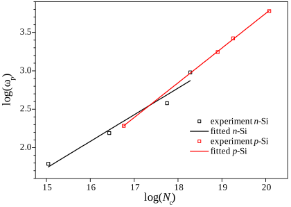
To study the likely differences in the electron
parameters of n- and p-doped silicon samples, the
corresponding experimentally obtained dependences of the
plasma frequencies on the carrier concentrations ωp(Nc) are
presented separately in Fig. 4(a). Here, a clear difference
between two straight lines corresponding to the linear
fitting of the logl-log wp(Nc) dependences for the n- and pdoped
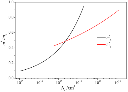
silicon samples is observed. Calculated dependences
of the effective electron masses on the carrier concentration,
m*
n(Nc) and m*
p(Nc) corresponding to these p(Nc)
dependences, are presented in Fig. 4(b). For the carrier
concentration of Nc < 2 · 1017 cm-3, the effective electron
mass is smaller than the effective hole mass, m*
n < m*
p
[Fig. 4(b)]. The latter agrees with the known reference data
for the conductivity effective mass in a silicon crystal,
m*
n = 0.27 and m*
p = 0.39 [24]. For the carrier
concentration of Nc > 2 · 1017 cm-3, the opposite relation
between the effective masses of m*
n > m*
p takes place
[Fig. 4(b)]. Such change of the sign of the effective mass
difference m*
n − m*
p with an increase of the carrier
concentration, Nc, is the consequence of crossing the
straight lines on the dependences log(ωp) on log(Nc)
[Fig. 4(a)]. Taking into account that the DFT calculated
dielectric permittivity of the heavily boron-doped silicon
crystals, ε∞ = 10.38, is smaller than the similar value for the
pure silicon, ε∞ = 11.46, the curve of the dependence
m*
p(Nc) in Fig. 4(b) will be shifted a bit to the larger
magnitudes of the effective mass, m*
p. Thus, one may
expect the relation of m*
n > m*
p to take place for the carrier
concentration a bit larger than the above-mentioned one
Nc > 2 · 1017 cm-3.
Fig. 4. (a) Log-log dependences of the plasma frequency ωp on the free carrier concentration Nc in the form of experimental points
(Table 2) and solid straight lines (linear fittings of the dependences ωp(Nc) in the form of experimental points) for the dopedsilicon
crystals; (b) dependences of the effective electron/hole masses m* on the logarithm of the carrier concentration Nc calculated
using the fitted data in Fig. 4(a) and (2). Black and red colours correspond to the n- and p-type doping of silicon crystals.
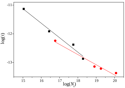
A clear increase of the damping coefficient γ with an
increase in the free carrier concentration Nc observed
(Table 2) is caused by a corresponding increase in the free
electron-electron interaction/scattering. The observed
inverse dependence of logarithm of the momentum
scattering time log(τ) (τ = 1/(γc), where c is the light
velocity on the logarithm of carrier concentration log(Nc)
(Fig. 5), is a result of this interaction. Therefore, the free
electron/hole momentum scattering time τ decreases by
two orders of magnitude when the free carrier
concentration Nc of the doped silicon crystals increases by
four orders of magnitude (Fig. 5). For relatively low free
carrier concentrations Nc < 1017 cm-3, the momentum
scattering times of free electrons are a bit larger than the
momentum scattering times of the holes (Fig. 5).
Fig. 5. Log-log dependences of the momentum scattering time τ
on the free carrier concentration Nc in the form of
experimental points (Table 2) and solid straight lines
(linear fittings of the dependences log(τ) on log(Nc) in the
form of experimental points) for the doped silicon
crystals.
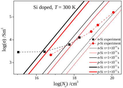
According to the theory of electron conductivity in
metals, the direct proportionality between the conductivity
σ and the carrier concentration Nc takes place if the
momentum scattering time τ and effective mass m* are
constant:
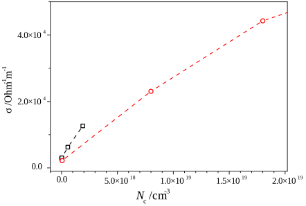
This, however, is not realized because a clear
nonlinearity of the dependences σn(Nc (n)) and σn(Np
(p)) is
observed: the relation τ/m* decreases with an increase of Nc [Fig. 6(a)]. This agrees with a relatively strong decrease of
the momentum scattering time τ (Fig. 5) and a moderate
increase of the effective mass m* [Figs. 3(a), 4(b)]. Thus,
the main reason for the observed nonlinearity of the
dependences σn(Nc (n)) and σn(Nc (p)) is a decrease of the
momentum scattering time τ with an increase in the carrier
concentration Nc. The same conclusion can be derived from
comparing the experimental and the theoretical dependences
σ(Nc) presented in log-log scales [Fig. 6(b)].
Fig. 6. (a) Dependences of the electric conductivity σ of silicon crystals on the free carrier concentration Nc corresponding to free electrons
(black colour) and holes (red colour) obtained from the FTIR experiment; (b) dependences of the electric conductivity σ on the
electron/hole concentration Nc in log-log scales for n- (black) and p-type (red) silicon crystals obtained from the FTIR experiment
(points and dashed lines) and calculated using the AMSET code within the constant relaxation time approximation (solid lines).
The RefFIT fitted parameters of the doped silicon
crystals presented in Table 2 were obtained using the model
of a silicon plane parallel plate of a finite thickness (silicon
crystals of a thickness of 0.45 mm) in vacuum. However, if
one uses the model of an infinitely thick slab, the fitted
parameter ε∞ obtained for the carrier concentrations less
than Nc = 1 · 1017 cm-3 is larger than those with concentrations
of Nc > 1 · 1017 cm-3. This is caused by an increase in
the reflection coefficient R due to the partial transparency
and back-side light reflection of the samples studied. The
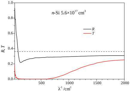
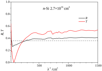
latter feature leads to an increase in the fitted parameter ε∞. Fig. 7 illustrates this effect. For the carrier concentration
of Nc = 5.6 · 1017 cm-3 [Fig. 7(a)], the transmittance T of the
sample is still relatively small and the light reflection is
realized mainly from the front surface of the sample. This results in a case where the measured reflection coefficient [solid black curve in Fig. 7(a)] is smaller than the calculated one based of the refractive index of the silicon single crystal n = 3.6 for the wavelength λ = 1 μm [22] (dashed horizontal line), corresponding to the range of silicon transparency. For the carrier concentration of Nc = 2.7 · 1016 cm-3 [Fig. 7(b)], the transmittance T of the sample is relatively high and the light reflection is additionally realized from the back-side of the sample surface. This, in turn, results in the opposite case where the measured reflection coefficient [(solid black curve in Fig. 7(b)] becomes larger than the calculated one [dashed horizontal line in Fig. 7(b)].
Fig. 7. Reflection and transmission spectra R(λ−1) and T(λ−1) of n-type-doped silicon single crystals for two carrier concentrations,
(a) Nc = 5.6 · 1017 cm-3 and (b) Nc = 2.7 · 1016 cm-3. Horizontal dashed line indicates the specular reflection coefficient R for the
normal incidence and corresponding to the refractive index of a silicon single crystal n = 3.6 for the wavelength λ = 1 μm [22].
Conclusions
By applying the Drude model of the frequency-dependent dielectric permittivity ε(ω) to the quasi-free electrons in the n- and p-doped silicon crystals of the carrier concentration in the range of 1015−1020 cm-3, the clear non-linear depend-ence of the square plasma frequency on the carrier concentration Nc is found. Analysis of this non-linearity reveals an increase in the electron effective mass m* with an increase of the carrier concentration Nc. The dependence m*(log(Nc)) is close to the linear one in the relatively wide carrier concentration range of 1015−1020 cm-3. For the relatively low free carrier concentrations of Nc < 1017 cm-3,
the electron effective masses m*n are smaller than the effective masses of the holes m*p.
For n- and p-doped silicon crystals studied, the free electron/hole momentum scattering time τ decreases more than two orders of magnitude when the free carrier concen-tration Nc increases in the range of 1015−1020 cm-3. For the relatively low free carrier concentrations of Nc < 1017 cm-3, the free electrons momentum scattering times are a bit larger than the momentum scattering times of the holes.
In the wide range of the carrier concentration Nc, the relation (5) between the electric conductivity σ and the free carrier concentration Nc in the doped silicon crystals is strongly nonlinear, which is revealed in a decrease of τ/m* with an increase of Nc. This concentration decrease of τ/m* is due to the simultaneous reduction in the momentum scattering time τ and the effective mass m* increase. At the same time, the corresponding relative decrease of the momentum scattering time |Δτ/τ| is approximately three times larger than the relative increase of the effective mass |Δm*/m*|. For the free carrier concentrations of Nc < 2 · 1018 cm-3, the free electron conductivity σn is larger than the hole electric conductivity σp, that is in agreement with the corresponding relations for the momentum scattering times (τn, τp) and the effective masses (m*n, m*p).
Using the DFT calculations of the band electronic structure of doped silicon crystals, it was found that: (1) the heavily n-type doping (Nc = 5 · 1022 cm-3), performed by the replacement of silicon atoms by the phosphorus atoms, leads to an increase in the dielectric permittivity ε∞ of the crystal by about 13%; (2) the heavily p-type doping (Nc = 5 · 1022 cm-3), performed by the replacement of silicon atoms with the boron atoms, leads to a decrease in the dielectric permittivity ε∞ of the crystal by approxi-mately 10%.
Authors’ statement
Research concept and design, A.B., L.B., N.A. and A.P.; collection and/or assembly of data, A.B., L.B., U.S., L.P., A.I.K. and A.V.; data analysis and interpretation, A.B., L.B., A.V., U.S., L.P. and A.I.K.; writing the article, A.B., L.B., N.A., U.S. and A.V.; critical revision of the article, A.P. and A.V.; final approval of article, A.B. and L.B.
Acknowledgements
Experimental measurements were performed with infrared synchrotron radiation at the IRIS beamline of the electron storage ring BESSY II at the Helmholtz-Zentrum Berlin für Materialien und Energie in the framework of the BESSY proposal 232-12203-ST. Computer calculations were performed at ICM of Warsaw University, Poland (projects nos. g93-1636 and g96-1832) and WCSS of Wrocław University of Science and Technology, Poland (project no. 053).
References
Tulsyan, G. Doping Profile Measurements in Silicon Using Terahertz Domain Spectroscopy (THz-TDS) Via Electrochemical Anodic Oxidation. (Rochester Institute of Technology, Rochester, N.Y., 2015).
Yoo, H., Heo, K., Ansari, H. R. & Cho, S. Recent advances in electrical doping of 2D semiconductor materials: Methods, analyses, and applications. Nanomaterials 11, 832 (2021). https://doi.org/10.3390/nano11040832
Lan, C.-W., Hsu, C. & Nakajima, K. 10-Multicrystalline Silicon Crystal Growth for Photovoltaic Applications. in Handbook of Crystal Growth: Bulk Crystal Growth, Second Edition (Ed. Rudolph, P.) II, 373–411 (Elsevier, 2015). https://doi.org/10.1016/B978-0-444-63303-3.00010-9
Du, L., Yin, J., Zeng, W. & Yi, H. First-principles calculations to investigate electronic structures and optical properties of chalcogens-hyperdoped silicon. Solid State Commun. 342, 114610 (2022). https://doi.org/10.1016/j.ssc.2021.114610
Marri, I., Degoli, E. & Ossicini, S. First principle studies of B and P doped Si nanocrystals. Phys. Status Solidi (A) Appl. Mater. Sci. 215, 1700414 (2018). https://doi.org/10.1002/pssa.201700414
Schade, U., Ortolani, M. & Lee, J. Technical Report: THz experiments with coherent synchrotron radiation from BESSY II. Synchrotron Radiat. News 20, 17–24 (2007). https://doi.org/10.1080/08940880701631351
Sólyom, J. Fundamentals of the Physics of Solids, Volume II: Electronic Properties. (Springer-Verlag Berlin Heidelberg, 2009). https://doi.org/10.1007/978-3-540-85316-9
Kuzmenko, A. B. Kramers-Kronig constrained variational analysis of optical data. Rev. Sci. Instrum. 76, 083108 (2005). https://doi.org/10.1063/1.1979470
Spitzer, W. G. & Fan, H. Y. Determination of optical constants and carrier effective mass of semiconductors. Phys. Rev. 106, 882–890 (1957). https://doi.org/10.1103/PhysRev.106.882
Kresse, G. & Hafner, J. Ab initio molecular-dynamics simulation of the liquid-metal-amorphous-semiconductor transition in germanium. Phys. Rev. B 49, 14251–14269 (1994). https://doi.org/10.1103/PhysRevB.49.14251
Kresse, G. & Furthmüller, J. Efficiency of ab-initio total energy calculations for metals and semiconductors using a plane-wave basis set. Comput. Mater. Sci. 6, 15–50 (1996). https://doi.org/10.1016/0927-0256(96)00008-0
Kresse, G. & Furthmüller, J. Efficient iterative schemes for ab initio total-energy calculations using a plane-wave basis set. Phys. Rev. B 54, 11169–11186 (1996). https://doi.org/10.1103/PhysRevB.54.11169
Kresse, G. & Joubert, D. From ultrasoft pseudopotentials to the projector augmented-wave method. Phys. Rev. B 59, 1758–1775 (1999). https://doi.org/10.1103/PhysRevB.59.1758
Madsen, G. K. H. & Singh, D. J. BoltzTraP. A code for calculating band-structure dependent quantities. Comput. Phys. Commun. 175, 67–71 (2006). https://doi.org/10.1016/j.cpc.2006.03.007
Riffe, D. M. Temperature dependence of silicon carrier effective masses with application to femtosecond reflectivity measurements., 1092–1100 (2002). https://doi.org/10.1364/JOSAB.19.001092
Naik, G. V., Shalaev, V. M & Boltasseva, A. Alternative plasmonic materials: Beyond gold and silver. Adv. Mater. 25, 3264–3294 (2013). https://doi.org/10.1002/adma.201205076
Chen, Y. B & Zhang, Z. M. Heavily doped silicon complex gratings as wavelength-selective absorbing surfaces. J. Phys. D 41, 095406 (2008). https://doi.org/10.1088/0022-3727/41/9/095406
Faruque, O., Al Mahmud, R. & Sagor, R. H. Heavily doped silicon: A potential replacement of conventional plasmonic metals. J. Semicond. 42, 062302 (2021). https://doi.org/10.1088/1674-4926/42/6/062302
Schroder, D. K. Semiconductor Material and Device Characterization, Third Edition. (John Wiley & Sons, Inc., 2006). https://doi.org/10.1002/0471749095